(Hong Kong)

Product Summary
SAK-C164SL-8RM The architecture of the C164CI combines advantages of both RISC and CISC
processors and of advanced peripheral subsystems in a very well-balanced way. In
addition the on-chip memory blocks allow the design of compact systems with maximum
performance.SAK-C164SL-8RM
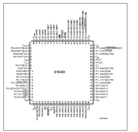
The following block diagram gives an overview of the different on-chip components and
of the advanced, high bandwidth internal bus structure of the C164CI.SAK-C164SL-8RM
Parametrics
Derivative1) Program CAPCOM6 CAN Interf Operating
Memory Frequency
SAK-C164CI-8R[25]M 64 KByte ROM Full function CAN1 20 MHz,
SAF-C164CI-8R[25]M [25 MHz]
SAK-C164SI-8R[25]M 64 KByte ROM Full function --- 20 MHz,
SAF-C164SI-8R[25]M [25 MHz]
SAK-C164CL-8R[25]M 64 KByte ROM Reduced fct. CAN1 20 MHz,
SAF-C164CL-8R[25]M [25 MHz]
SAK-C164SL-8R[25]M 64 KByte ROM Reduced fct. --- 20 MHz,
SAF-C164SL-8R[25]M [25 MHz]
SAK-C164CL-6R[25]M 48 KByte ROM Reduced fct. CAN1 20 MHz,
SAF-C164CL-6R[25]M [25 MHz]
SAK-C164SL-6R[25]M 48 KByte ROM Reduced fct. --- 20 MHz,
SAF-C164SL-6R[25]M [25 MHz]
SAK-C164CI-L[25]M --- Full function CAN1 20 MHz,
SAF-C164CI-L[25]M [25 MHz]
SAK-C164CI-8EM 64 KByte OTP Full function CAN1 20 MHz
SAF-C164CI-8EM
Features
1.High Performance 16-bit CPU with 4-Stage Pipeline
–80 ns Instruction Cycle Time at 25MHz CPU Clock
–400 ns Multiplication (16 × 16 bit), 800 ns Division (32 / 16 bit)
–Enhanced Boolean Bit Manipulation Facilities
–Additional Instructions to Support HLL and Operating Systems
–Register-Based Design with Multiple Variable Register Banks
–Single-Cycle Context Switching Support
–16 MBytes Total Linear Address Space for Code and Data
–1024 Bytes On-Chip Special Function Register Area
2.16-Priority-Level Interrupt System with 32 Sources, Sample-Rate down to 40 ns
3.8-Channel Interrupt-Driven Single-Cycle Data Transfer Facilities via
Peripheral Event Controller (PEC)
4.Clock Generation via on-chip PLL (factors 1:1.5/2/2.5/3/4/5),
via prescaler or via direct clock input
5.On-Chip Memory Modules
–2 KBytes On-Chip Internal RAM (IRAM)
–2 KBytes On-Chip Extension RAM (XRAM)
–up to 64 KBytes On-Chip Program Mask ROM or OTP Memory
6.On-Chip Peripheral Modules
7.High Performance 16-bit CPU with 4-Stage Pipeline
–80 ns Instruction Cycle Time at 25MHz CPU Clock
–400 ns Multiplication (16 × 16 bit), 800 ns Division (32 / 16 bit)
–Enhanced Boolean Bit Manipulation Facilities
–Additional Instructions to Support HLL and Operating Systems
–Register-Based Design with Multiple Variable Register Banks
–Single-Cycle Context Switching Support
–16 MBytes Total Linear Address Space for Code and Data
–1024 Bytes On-Chip Special Function Register Area
8.16-Priority-Level Interrupt System with 32 Sources, Sample-Rate down to 40 ns
9.8-Channel Interrupt-Driven Single-Cycle Data Transfer Facilities via
Peripheral Event Controller (PEC)
10.Clock Generation via on-chip PLL (factors 1:1.5/2/2.5/3/4/5),
via prescaler or via direct clock input
11.On-Chip Memory Modules
–2 KBytes On-Chip Internal RAM (IRAM)
–2 KBytes On-Chip Extension RAM (XRAM)
–up to 64 KBytes On-Chip Program Mask ROM or OTP Memory
12.On-Chip Peripheral Modules
13.Supported by a Large Range of Development Tools like C-Compilers,
Macro-Assembler Packages, Emulators, Evaluation Boards, HLL-Debuggers,
Simulators, Logic Analyzer Disassemblers, Programming Boards
14.On-Chip Bootstrap Loader
15.80-Pin MQFP Package, 0.65mm pitch
Diagrams
 |
 SAK-164CI-8EM |
Other |
|
Data Sheet |
Negotiable |
|
||||||||||
|
SAK-90 |
|
KIT ARM-ASSY FOR SA9 TO SA90 SER |
Data Sheet |
|
|
||||||||||
 |
SAK-C161CS-LF CA |
Infineon Technologies |
16-bit Microcontrollers (MCU) MICROCONTROLLER 16-BIT |
Data Sheet |
|
|
||||||||||
|
SAK-C161JC-LF CA |
Infineon Technologies |
16-bit Microcontrollers (MCU) MICROCONTROLLER 16-BIT |
Data Sheet |
|
|
||||||||||
|
SAK-C164CI-8E25M DB |
Infineon Technologies |
16-bit Microcontrollers (MCU) 16-Bit Sngl-Chip 5V 25MHz OTP |
Data Sheet |
Negotiable |
|
||||||||||
|
SAK-C164CI-8EM CB |
Infineon Technologies |
16-bit Microcontrollers (MCU) 16 BIT OTP |
Data Sheet |
Negotiable |
|
||||||||||