(Hong Kong)

Product Summary
The 512-Mb DDR2 DRAM is a high-speed Double
Data-Rate-2 CMOS Synchronous DRAM device
containing 536,870,912 bits and internally configured
as a quad-bank DRAM. The 512-Mb device i
organized as either 32Mbit × 4I/O × 4banks, 16Mb
× 8I/O × 4banks or 8Mbit × 16I/O × 4banks chip
These synchronous devices achieve high speed
transfer rates starting at 400Mb/sec/pin for genera
applications. See Table3 for performance figures.
The device is designed to comply with all DDR2 DRAM
key features:
1.posted CAS with additive latency,
2.write latency = read latency -1,
3.normal and weak strength data-output driver,
4.Off-Chip Driver (OCD) impedance adjustment
5.On-Die Termination (ODT) function.
All of the control and address inputs are synchronized
with a pair of externally supplied differential clocks.
Inputs are latched at the cross point of differential
clocks (CK rising and CK falling). All I/Os are
synchronized with a single ended DQS or differential
DQS-DQS pair in a source synchronous fashion.
A 16-bit address bus for ×4 and ×8 organised
components and a 15-bit address bus for ×16
components is used to convey row, column and bank
address information in a RAS-CAS multiplexing style.
The DDR2 device operates with a 1.8V ± 0.1V power
supply. An Auto-Refresh and Self-Refresh mode is
provided along with various power-saving power-down
modes.
The functionality described and the timing
specifications included in this data sheet are for the
DLL Enabled mode of operation.
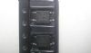
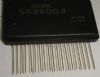
The DDR2 SDRAM is available in P-TFBGA package.
Parametrics
Product Type Speed Code –3S Unit
Speed Grade DDR2–667D 5–5–5 —
max. Clock Frequency @CL5 fCK5 333 MHz
@CL4 fCK4 266 MHz
@CL3 fCK3 200 MHz
min. RAS-CAS-Delay tRCD 15 ns
min. Row Precharge Time tRP 15 ns
min. Row Active Time tRAS 45 ns
min. Row Cycle Time tRC 60 ns
Features
HYB18TC512160AF-3S
1.8 V ± 0.1 V Power Supply
1.8 V ± 0.1 V (SSTL_18) compatible I/O
DRAM organisations with 4, 8 and 16 data
in/outputs
HYB18TC512160AF-3S
Double Data Rate architecture: two data transfers
per clock cycle, four internal banks for concurrent
operation
CAS Latency: (2), 3, 4 and 5
Burst Length: 4 and 8
Differential clock inputs (CK and CK)
Bi-directional, differential data strobes (DQS and
DQS) are transmitted / received with data. Edge
aligned with read data and center-aligned with write
data.
DLL aligns DQ and DQS transitions with clock
DQS can be disabled for single-ended data strobe
operation
Commands entered on each positive clock edge,
data and data mask are referenced to both edges of
DQS
Data masks (DM) for write data
Posted CAS by programmable additive latency for
better command and data bus efficiency
Off-Chip-Driver impedance adjustment (OCD) and
On-Die-Termination (ODT) for better signal quality.
Auto-Precharge operation for read and write bursts
Auto-Refresh, Self-Refresh and power saving
Power-Down modes
Average Refresh Period 7.8 μs
Full and reduced Strength Data-Output Drivers
1K page size for ×4 & ×8, 2K page size for ×16
Packages:
P-TFBGA-60 for ×4 & ×8 components
P-TFBGA-84 for ×16 components
RoHS Compliant Products1)
Diagrams

 |
 HYB18T512800BF-3.7 |
|
IC DDR2 SDRAM 512MBIT 60TFBGA |
Data Sheet |
Negotiable |
|
||||||
 |
HYB18T512800BF-3S |
|
IC DDR2 SDRAM 512MBIT 60TFBGA |
Data Sheet |
|
|
||||||
 |
HYB18T256324F20 |
Other |
|
Data Sheet |
Negotiable |
|
||||||
|
HYB18T256161BF-25 |
Other |
|
Data Sheet |
Negotiable |
|
||||||
|
HYB18T256161BF-20 |
Other |
|
Data Sheet |
Negotiable |
|
||||||
|
HYB18T256160AFL-3.7 |
Other |
|
Data Sheet |
Negotiable |
|
||||||